The Challenges of IoT in PCB Design and Manufacturing
A survey of the challenges in manufacturing and design of IoT from the design step to the production stage
Introduction
The Internet of Things (IoT) devices aren’t just regular electronic products, but a special breed of printed circuit boards (PCBs) that push the boundaries of manufacturers and designs. In fact, the manufacturers of these devices are having a hard time keeping up with the massive introductions of new technologies on the market. IoT devices are subject to strict design rules and complicated component integration while technology is constantly evolving, so manufacturers have to accommodate these impacts.
IoT (Internet of Things) technology has been slowly being adopted by many companies and organizations and it’s estimated that more than half of them find it challenging. Some IoT projects didn't make it to market. For example, according to a 2017 Cisco report, at least 74 percent of IoT projects fail. Nevertheless, there is still a huge driving force from market needs, the production of smart IoT devices on the market has increased significantly.
It's important to understand the effects of IoT on PCB manufacturing if you want to have successful IoT projects.
Understanding the Unique Needs of IoT Manufacturing
The Internet of things is aiming to connect and network devices, appliances, and possibly any object in order to improve operations, processes, maintenance, or to offer new features or services.
IoT devices are becoming more complex and high-tech as they require embedding a wireless connectivity solution to enable them to communicate with each other. Interoperable among different telecommunication and wireless technologies, including LTE, 5G, LoRa, BLE, Sub 1 GHz, Wi-Fi, ZigBee, and NB-IoT, can become very challenging in real-world implementations.
Challenge 1: Embedding wireless communication technology
One of the challenges of IoT in PCB design and manufacturing lies in the need of embedding wireless communication capabilities into the myriad of smart objects that are on the market today. Adding radio frequency (RF) components to the design of a product introduced stricter design rules to the overall system, including the printed circuit board. To ensure that products don't cause any transmission losses and interference issues, they must go through different quality control tests during their manufacturing process.
Challenge 2: Integration
Another challenge of the manufacturing and design of IoT is the integration of various components and the way of fitting into a compact form factor. Some companies provide integrated modules that allow the complete cellular communication capability to be prepackaged in a single component. In this way, Cellular IoT modules incorporate baseband radio frequency (RF) chips and other useful functionalities. These modules are usually certified where it belongs to a form factor family, which can reduce the compliance burden significantly, and leverage a single product design to deploy across various regions. One must not overlook the importance of this challenge in the product design phase.
Placement and routing are the two main steps in the design of PCB and integrated circuits (IC). In the first step, we need to decide on the locations of the electronic components to be placed. The next step is to connect among these electronic elements called the routing step, where it must follow the strict rules and limitations of the manufacturing process.
An important factor that affects routing is the choice of the stack-up, that is the number and type of layers that make up the printed circuit. RF PCBs consist of 2 or 4 layers. But in some cases, they can go up to 8 layers. An extra layer of circuit board improves routing, provides a separate ground plane for components, and allows for both power and ground planes.
The PCB designer must ensure that the PCB is well isolated from unwanted electromagnetic interference (EMI)/radio-frequency interference (RFI), and therefore, needs to ensure that the required radio signals are properly isolated from unwanted signals. The common practice is to use a solid (uninterrupted) ground plane, placed immediately below the upper layer where components and transmission lines are placed.
On top of PCB routing, the design team must take extra care to make sure there is no radio frequency (RF) crosstalk problems between the RF circuitry and the baseband section. Lastly, the testing processes most likely require RF testers on the line which will not be forgotten.
Challenge 3: Manufacturability
Another challenge is the Design for Manufacturability (DFM) since designing and manufacturing products are two different stories. In manufacturing, you need to consider factors such as overall costs, raw material, the form of the raw material, dimensional tolerances, and secondary processing such as in a typical SMT (Surface Mount Technology) process. Often design teams look at DFM as a “manufacturing problem” but, it may be an oversight issue especially since one cannot imagine the dimensional space constraint when a component is bendable having weird angles. Thus, most manufacturers will perform DFM analysis prior to production to identify and fix manufacturing issues [See Figure: Collusion detection]. However, we should not rely on manufacturers to catch the issues, but rather performing our own analysis prior to the prototype could have detected those same issues and altered them in engineering. Doing so would have lowered the cost and unnecessary back-and-forth tries and corrections between your design teams and the manufacturers.
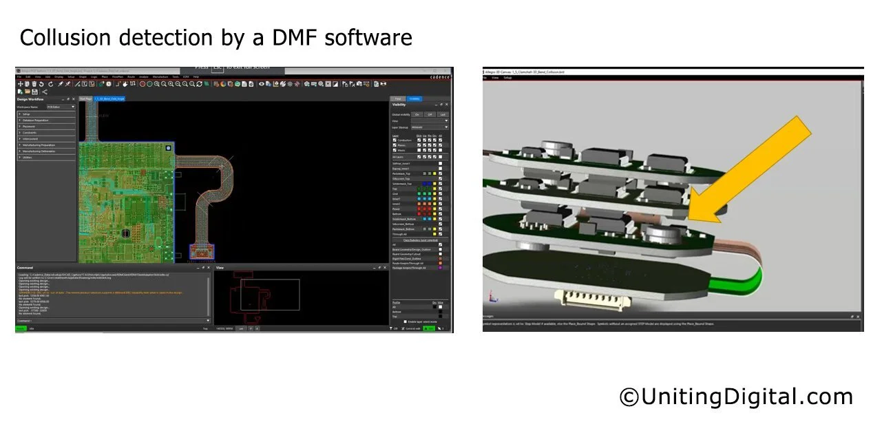
Collusion detection by a DMF software [Using Cadence as shown here]
There are many DMF software available in the market. Here are some examples of DMF analysis software:
Challenge 4: Management of BOM and Supply Chain
Besides the actual design and manufacturing challenges, there are many practical challenges that contribute to the failure of IoT projects to make them to the market, such as supply chain management, BOM management, and software tools.
The challenge in supply chain management is no news but because of COVID-19 and the rapid demand from the electronics industry, unpredictability and disruption are running high when it comes to the overall industry supply chain. Companies need to create realistic supply chain strategies and ways of obtaining the latest information about component specifications, CAD libraries (https://www.ultralibrarian.com/), and establish and optimize the supply chain structure including forecasting, demand planning, and fulfillment, supplier scheduling, deployment, and strategic sourcing.
Supply chain issues are always there. Companies need to have effective ways of controlling the BOM, which includes using the right software tools and continuing to check the availability of certain key components throughout the entire design process even before building the prototype. Keeping up to date with rev controls on the BOM, drawings, and schematics is a survival skill, especially for IoT projects. Most importantly, we need to keep good relationships between our buyers and suppliers that gear toward mutual benefit by showing genuine concerns, keeping a reliable open dialogue, and forging a trusting relationship.
Challenge 5: Production
Finally, working with your PCB assembly shop is another challenge in the manufacturing and design of IoT in the final step. Even when we have eliminated all DFM issues, we still need to manage carefully with your PCB assembly shops. To meet the timeline of production, we need to manage the availability of the assembly line, parts, and materials in special processes carefully. Having a flexible strategy and knowing realistic on the leading time on various factors including tooling, fixtures, or special processes that are not in the BOM, are key to having successful product manufacturing. Tooling may become a trouble for the inexperienced ones because it is not in the BOM, and it has its own timeline and availability. The tooling size and weight could also affect the delivery and thus cause unnecessary delays in the shipping process.
Conclusion
We have quickly presented a survey of the challenges in manufacturing and design of IoT from the design step to the production stage. There are certain risks coming from various factors such as manufacturability, supply-chain disruptions, and processes management in all steps. In the design phase, we also need to understand certain technology trade-offs where they could affect the overall size, flexibility in design and manufacturing, the time required if it needs to be handmade, etc. From the DMF analysis, we learned that routine collision detection and identification of rule violations help check the design before sending it to manufacturing. You may discover heating issues on the board ahead of time with the appropriate software tool since the smaller its design in terms of space increases its complexity many more folds, which leads to more error prone. As a result, having the right set of software tools is especially important for IoT projects. Finally, establishing a great revision process for BOM management is crucial for any successful IoT project.
About the Author
Arthur Wang